
Silicon Photonics Chips for AI Infrastructure
Silicon Photonics Chips are transforming AI infrastructure by using optical interconnects for faster, low-interference data transfer. This guide explains how the technology works, its key applications, and why it is becoming critical for data centers and high-performance computing.

TL;DR Silicon Photonics Chips move data with optical interconnects instead of only electrical traces, which makes them important for AI infrastructure, data centres, and dense chip integration.
Understanding Silicon Photonics Technology
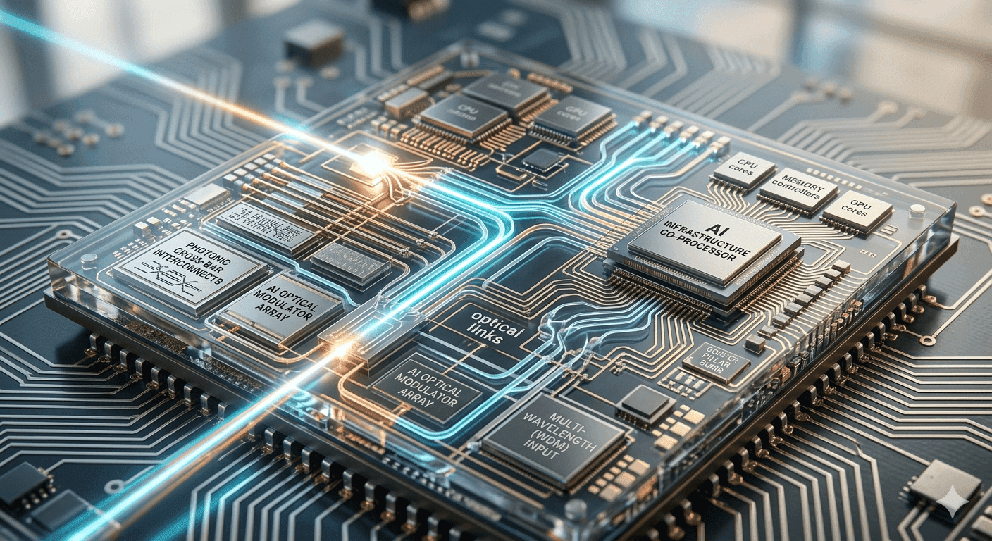
Silicon photonics is entering a new era of large-scale integration, with 500 to 10,000 components on the same chip. That scale is the main reason Silicon Photonics Chips matter now, because it turns optical links into integrated systems instead of one-off parts. At a basic level, silicon photonics is a platform for building photonic integrated circuits for optical communication, high-speed data transfer, and photonic sensing devices.
In plain terms, the technology puts light-handling functions on silicon, then ties them to electronic control where required. That mix is what makes the platform practical for real applications. The phrase what is silicon photonics comes up a lot because the answer is simple and useful. It is integrated photonics on silicon, usually built on a silicon on insulator substrate, with silicon oxide used as cladding and buffer layers.
That material stack matters because the refractive index contrast helps confine light inside waveguides. Silicon photonics companies keep pushing this model because it fits existing semiconductor manufacturing processes. Intel and other silicon chip companies have spent years showing that optical and electronic functions can coexist in the same package. The result is not a science demo; it is a manufacturing strategy for high-volume production.
In this architecture, optics and electronics work together on the same substrate, which helps keep the design compact and practical. The real advantage is not just speed; it is integration. Silicon photonics chip design lets a single substrate carry waveguides, lasers, modulators, and detectors in a tightly integrated layout.
That reduces the distance data must travel through electrical circuits, which lowers delay and helps performance at scale. This is also why the technology is useful for optical communication and optical coupling. A single optical path can carry more data through fibre than a short copper trace can handle cleanly, especially when systems grow denser.
If you are building AI servers or cloud fabrics, that difference becomes obvious fast. The laser and waveguide path are part of what makes the layout efficient, while the low-loss routing keeps the system practical. Silicon photonics enabled chip based 3d printer concepts, optical networking, and sensing all depend on the same core idea, which is moving light through integrated structures with less loss.
The platform is also being used in applications such as LIDAR, image projection, photonic switching, and programmable circuits. Those applications show why the technology is not locked into one market. The practical gain is that optical data transfer can happen without the same electromagnetic interference problems that conventional electrical links face.
That matters in crowded racks, dense boards, and mixed-signal systems. It also matters when a design needs stable power performance through long fibre runs or through tightly packed devices. In these systems, low interference and compact optics are key advantages.
- Silicon photonics is built for optical interconnects, not just short internal links.
- Silicon photonics companies favour it because the manufacturing path can scale.
- Silicon chip companies use it to move light where copper starts to struggle.
Key Applications Driving Adoption
Silicon photonics technology is used across several application areas, and that breadth is part of its appeal. Optical communication remains the most direct fit because the platform was built to move data quickly and cleanly. High-speed data transfer, optical networking, and photonic switching all benefit from the same low-loss routing and compact integration.
The technology also extends into sensing, LIDAR, image projection, and programmable circuits. Those use cases show that the platform is not limited to one type of system design. In each case, the value comes from putting optical functions on silicon while keeping the package compact enough for practical deployment.
Why Silicon Photonics Chips Matter for AI Infrastructure
Silicon Photonics Chips are especially relevant for AI infrastructure because they support the kind of dense, high-speed data movement that large systems demand. The article already shows why this matters: silicon photonics can scale to 500 to 10,000 components on a single chip, and that level of integration helps turn optical links into practical system-level building blocks.
In AI servers and cloud fabrics, that means optical interconnects can help reduce delay, lower interference, and keep performance practical as systems get denser. The same design advantages also make the technology attractive for data centers and mixed-signal environments. Optical data transfer avoids many of the electromagnetic interference issues that conventional electrical links face, and that is useful in crowded racks and tightly packed devices.
As silicon photonics companies continue pushing manufacturing-scale integration, the technology is positioned as a practical path for high-volume optical connectivity. If you are evaluating infrastructure for AI workloads, this is the point to watch closely. The strongest case for adoption comes when dense systems need both compact integration and cleaner signal paths.
Who Should Consider Silicon Photonics Chips
Silicon Photonics Chips make the most sense for teams building AI servers, cloud fabrics, and dense data centre systems. Those environments need fast data movement, and they also need a way to manage interference as racks and boards become more crowded. The technology fits that problem because it combines optical interconnects with semiconductor-style integration.
It is also a strong fit for groups working on optical communication, photonic switching, and sensing platforms. The same core architecture supports LIDAR, image projection, and programmable circuits, so the technology has room beyond one narrow use case. If your project depends on compact layouts and low-loss routing, the platform deserves serious attention.
For smaller systems that do not face heavy bandwidth pressure, the benefits may be less urgent. In that case, conventional electrical links can still be easier to deploy. The key question is whether your system needs the scale and density that make optical integration worthwhile.
Frequently Asked Questions
Q. What makes Silicon Photonics Chips different from ordinary electronic chips?
Silicon Photonics Chips combine optical functions with electronic control on the same substrate. The article notes that they can integrate 500 to 10,000 components on one chip, which is a major step beyond simple electrical traces. That integration helps move data through waveguides, lasers, modulators, and detectors in a compact layout.
Q. Why are Silicon Photonics Chips useful in AI infrastructure?
They matter because AI servers and cloud fabrics need dense, high-speed data movement. The article explains that optical interconnects can reduce delay and lower interference in crowded racks and tightly packed devices. That makes the technology practical for large systems where copper starts to struggle.
Q. What materials are commonly used in silicon photonics?
The article says the platform is usually built on a silicon on insulator substrate. It also mentions silicon oxide as cladding and buffer layers. That material stack helps confine light inside waveguides because of the refractive index contrast.
Q. What applications beyond AI can use this technology?
The article lists optical communication, high-speed data transfer, photonic sensing devices, LIDAR, image projection, photonic switching, and programmable circuits. It also mentions optical networking and sensing as practical uses. That range shows the platform is not limited to one market.
Q. Why does optical data transfer help in dense systems?
Optical data transfer avoids many electromagnetic interference problems that conventional electrical links face. The article says that matters in crowded racks, dense boards, and mixed-signal systems. It also helps when long fiber runs or tightly packed devices need stable performance.
Is Silicon Photonics Worth Watching for AI and Data Centers
Silicon Photonics Chips are worth watching because they combine optical interconnects with a manufacturing path that can scale. The article points to 500 to 10,000 components on a single chip, and that level of integration is what makes the technology relevant for AI infrastructure and data centers. It also helps explain why the platform keeps showing up in optical communication, photonic switching, and other high-density applications.
For AI server builders and cloud teams, the strongest reason to pay attention is the mix of compact integration and lower interference. For data center planners, the appeal is similar, since crowded racks and mixed-signal environments benefit from cleaner signal paths. For smaller projects, the technology may be more than you need right now, but it still sets a direction for future system design.
The clearest next step is to evaluate whether your workload needs optical interconnects at scale. If your system is already pushing density, bandwidth, or interference limits, this platform deserves a closer look. If not, it is still useful to understand because it is shaping how high-volume connectivity is built.


